Plasma Treatment to Create a Hydrophilic Surface on Silicon Substrates
See test below showing the initial contact angle of 45 to 74 degrees – after plasma treatment in the AutoGlow 1000 the contact angle was < 2 degrees.
Water-Drop-Testing:

contact angle of 48.69 degrees before Ar+H2 treatment

contact angle of 1.057 after plasma treatment using Ar+H2
Plasma Treatment to Create a Hydrophilic Surface on Silicon Substrates–is used to modify silicon wafer surface properties to make the surface hydrophilic–this improves the bond strength for subsequent processing. This process involves exposing the silicon substrate to a low-pressure plasma environment, typically utilizing gases such as oxygen or a argon/hydrogen mixture. Through the interaction between plasma species and the silicon surface, a chemical reactions occurs, leading to the formation of hydrophilic functional groups, primarily hydroxyl (-OH) moieties, on the surface.
Plasma-induced surface modification proceeds through sequential steps. Initially, energetic plasma species, including ions, electrons, and radicals, impact the silicon surface, breaking surface bonds–forming reactive species like silicon radicals and dangling bonds. Subsequently, these species react with surrounding gas molecules, predominantly oxygen or hydrogen, resulting in the incorporation of oxygen or hydrogen atoms onto the silicon surface.

initial contact angle prior to plasma treatment with O2 was 49.43

Contact angle of 1.257 after plasma treatment with O2
Introduction of these functional groups, notably hydroxyl (-OH) groups, alters the silicon wafer’s surface chemistry, rendering it hydrophilic. Hydroxyl groups exhibit a strong affinity for water molecules due to their polar nature, facilitating water adsorption and enhancing surface wetting. This transition from hydrophobic to hydrophilic surfaces holds significant importance in various technological domains, notably microfluidics, where precise control over surface wettability is vital for fluid manipulation and bioanalytical applications.
Plasma treatment offers notable advantages, including tunability, reproducibility, and scalability, making it ideal for integration into industrial manufacturing processes. Parameters such as gas composition, pressure, power density, and treatment duration can be finely adjusted to achieve desired surface properties with high precision and control. Furthermore, the non-destructive nature of plasma treatment preserves the bulk properties and structural integrity of the silicon substrate, maintaining its electronic and mechanical characteristics.
In semiconductor manufacturing, plasma treatment is particularly relevant for enhancing adhesion between silicon surfaces and functional layers like dielectric films or photoresists, thereby improving device performance and reliability. The ability to tailor surface properties at the nanoscale level enables the fabrication of advanced nanostructures and surface patterns, paving the way for the development of innovative electronic and photonic devices.
In conclusion, plasma treatment stands as a versatile and effective technique for engineering hydrophilic surfaces on silicon wafers, offering precise control over surface chemistry while preserving material integrity. Its wide applicability across diverse industries underscores its significance as a fundamental tool for advancing surface science and technology.
Plasma treatment is a sophisticated methodology, offering unparalleled precision in tailoring silicon wafer surfaces. Our test show results to increase the hydrophilic surfaces by reducing contact angles. Plasma treatment plays a pivotal role in various applications such as increasing bonding strength.
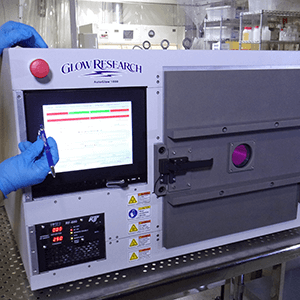
Testing was performed on the AutoGlow 1000 plasma system configured for RIE and Direct Plasma. RIE results are below.
RIE Configuration:
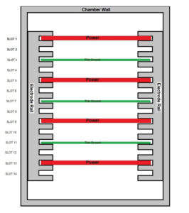
– One set of active/ground shelves (ground electrode shelf on top and powered electrode on bottom)
– For each process gas and power/pressure parameters
-collect 5 witness coupons. Measure initial sessile water contact angle
-load these 5 witness coupons to active electrode (see below pattern)
-set gas flow and throttle valve to attain given pressure conditions (computer control)
-process coupons at given power and time =300 seconds
-verify process power can with little to no reflected power (<5 watts)
-record sessile water contact angle of all 5 coupons
Direct Plasma Configuration:
-Add 2nd set of active/ground shelves (powered electrode on top and ground electrode on bottom)
-Repeat test as above
Achieving Hydrophilic Surfaces
A prominent application of plasma treatment on silicon wafers is the creation of hydrophilic surfaces. By subjecting the silicon substrate to a carefully orchestrated plasma environment—typically comprising oxygen or hydrogen gases—hydrophilic functional groups, notably hydroxyl (-OH) moieties, are seamlessly incorporated onto the surface. This augmentation fosters a heightened affinity for water molecules, thereby augmenting surface wettability and adhesion in critical technological endeavors.
Microfluidic Applications
The strategic advantages conferred by hydrophilic surfaces are used across a spectrum of industrial domains. In microfluidics, for instance, precise control over surface wettability is paramount for optimizing fluidic dynamics and analytical accuracy. Hydrophilic silicon wafers facilitate efficient fluid transport, mitigate surface tension effects, and bolster the reliability and reproducibility of microfluidic systems.
Contact Angle Reduction
Beyond facilitating hydrophilicity, plasma treatment can effectively reduce contact angles on silicon surfaces. This feat is achieved by finely tuning plasma parameters—such as gas composition, pressure, and treatment duration—to modulate surface energy and wetting behavior. Substantial reductions in contact angles enhance surface adhesion and compatibility with coatings, adhesives, and additional surface treatments. (see test results below)
Below is a short summary of the testing on the AutoGlow 1000. Contact Glow Research for more details and discussion—click HERE.
| Contact Angle on initial Si coupon | Sessile Water Contact Angle on Si after RIE Plasma
|
||||||||
| Gas | Pressure (mT) | Set Power (W) | Reflected Power (W) | Initial | 1 | 2 | 3 | 4 | 5 |
| O2 | 300 | 300 | 0 | 74.13 | 1.19 | 1.1 | 1.224 | 1.37 | 1.71 |
| Ar/H2 | 300 | 300 | 0.02 | 48.69 | 1.06 | 1.06 | 1.9 | 1.88 | 2.32 |
- Five silicon substrates were processed per run
- Five silicon substrates were positioned in the plasma chamber in the: (1)back-left, (2) back-right, (3) center, (4) front left and (5) front right

The Theta Light was used to measure contact angle. Provided by NanoScience Attension® Theta Lite Tensiometer
For information on the Theta Light above click HERE
For information on the AutoGlow 1000 click: https://www.glowresearch.org/autoglow-1000-production-plasma-cleaner/

AutoGlow production plasma system used for etching, cleaning and surface activation

AutoGlow 1000 chamber with 7 electrode shelves
