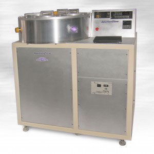
 System for Thin Film, Sputter, PVD, Thin Film Deposition, Vacuum Coating, Metallic or Dielectric Thin Film Deposition.
The Glow Research SputterGlow is a flexible sputter deposition system designed to process 200mm wafers, 156mm x 156mm solar cells or smaller wafers–including pieces of wafers. The SputterGlow can have up to three interchangeable process stations (each station can be configured for heating, sputter deposition or sputter etching). The SputterGlow was originally designed to deposit Si3N4 antireflective coatings on photovoltaic cells and can be used to sputter deposit a wide range of dielectrics or metals.
Photovoltaic engineers have found the SputterGlow to be an excellent alternative to Plasma Enhanced Chemical Vapor Deposition (PECVD) because the SputterGlow process does not require Silane (SiH4) for nitride deposition.
Along with the tremendous cost savings–of not requiring expensive facilitation or safety hurdles–many researchers feel there are strong advantages to using a sputtered film for the final passivation/anti-reflective coating, resulting in a higher efficiency photovoltaic cell.
Flexibility
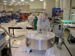
With three chamber stations, the SputterGlow can be used for a variety of processing needs. The individual stations can be interchangeably used for heating, sputtering or etching with proper choice of options at purchase, or retrofitted at a later date. The SputterGlow is a perfect choice for research or low volume manufacturing applications.
Chamber Integrity/cost

Vacuum Testing
The SputterGlow was designed to ensure process vacuum integrity and utilize an aluminum chamber (to keep cost down). The chamber has been helium leak tested to 6.5 x 10⁻¹⁰ mbar with all ports blocked, (4.8 x 10⁻¹⁰ torr).
The custom designed aluminum chamber allows for a 3X price reduction when compared to a stainless steel chamber of the same caliber. The SputterGlow can operate from an extremely low power of 25 watts (for less aggressive processing), to 1 kW for more aggressive sputter deposition.
The custom designed aluminum chamber allows for a 3X price reduction when compared to a stainless steel chamber of the same caliber. Chamber is 34” in diameter x 11” tall.
Proprietary Design
A proprietary planar magnetron is used to generate the plasma. This design results in a longer lifetime for the sputtering target, and improved deposition uniformity on the substrate. The Glow Research proprietary planar magnetron will also enhanced sputtering rates and lower heat transfer to the substrate.
PC Computer Control

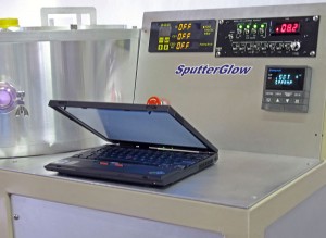
- Manual or Lap-Top Computer Control
An embedded microprocessor controls the motors of the wafer transport system, position of the wafer pedestals, opening of the vacuum and gas valves, etc. The user controls the deposition process by downloading a recipe from their personal laptop (not supplied). The embedded microprocessor is connected to the laptop via a USB port. The user can tailor their own process with the Glow Research proprietary sequencing program, or select any preset process that has been downloaded to their computer.
Power Supplies
The SputterGlow can be configured with RF, DC or pulsed DC power supplies. The SputterGlow can be used to deposit a variety of materials…dielectrics, semiconductors, metals and magnetic materials. Pulsed DC can be used instead of an RF supply with the advantage of eliminating the tuning network. A DC supply can specified if metals or magnetic materials are to be sputtered exclusively.
Background of the SputterGlow
SputterGlow Development: Production of the SuptterGlow plasma sputter deposition system started in 2010, with the goal of supplying the R&D market with a reasonably priced sputter deposition system for dilectrics and metals. Our first Customer, Arizona State University, needed a system to deposit nitride for a solar cell application. John Reche, with a long history of building sputtering systems, has led the design and manufacturing team with his ideas and experience. John has many years of experience in sputtering, photolithography, related microelectronics fabrication processes and thin-film optics.
Here is some background on John Reche:
John started development projects using polyimides as dielectrics for thin-film products. At the time, work with polyimides was limited to a few large research labs such as RCA, Bell Labs, IBM, TI or Hitachi that applied for a patent using PIQ (Poly-Isoindolo-Quinazolinedione) as ILD (Inner Layer Dielectric) to build bipolar integrated circuits. Since then, John has worked with dozens of commercial or experimental polyimides, as well as many other types of high temperature polymers.
John set-up his first complete sputtering and photolitho thin film R&D processing lab at GTE-Lenkurt in Vancouver, Canada. In this lab, he built experimental circuits using polyimide as cross-over dielectric. These circuits combined thick and thin-film hybrid technologies and flip-chip semiconductors supplied by Cherry’s and Motorola. The purpose of the experiment was to provide a simple and reliable interlayer dielectric for two-layers interconnects.
Later, John joined the magnetic thin-film head development group of Memorex in Santa-Clara (CA), where his responsibilities included developing polyimide insulated copper coils and finding a suitable ceramic material as substrate. Alumina titanium carbide was selected because it was the only non-porous material machinable, albeit with some difficulties, since its only use at the time was to make tool bits for metal machining.
John has built thin-film flip-chip memory modules with four polyimide layers and four interconnect copper layers for Hughes Aircraft Electro-Optics Division. This work led to the planning of a multichip module company.
His thin-film work led to building half a dozen clean rooms, sputtering equipment and control software for the machines. He also worked in thin-film optics, magneto-optics for data recording, and built Nd-Yag lasers. His thesis goal was to explore the fabrication of eeproms based on trapping charges between two dielectric layers. The dielectric layers were obtained by plasma anodizing a thin layer of aluminum deposited over silicon. Plasma anodization proceeded until all the aluminum formed a stoichiometric aluminum oxide with a thin layer of silicon anodized below it.
John holds seven US patents and three international patents. He authored over 60 technical papers and presentations at technical meetings. John obtained a Bachelor and a Master of Applied Sciences in Electrical Engineering from the University of British Columbia in Vancouver, Canada. His thesis was entitled: “The Preparation And Properties of rf-Plasma Anodized SiO2 & Al2O3 Thin Films and Al-Si Schottky Photodiodes”.
