Plasma Etching of Silicon Nitride (Si3N4) for RIE Removal for Failure Analysis
The goal was to remove the nitride layer on de-lidded semiconductor parts for oxide coverage inspection. Further goal was not to etch down to the metal layer. Below is the SEM shot showing the stack-up of the part with various device layers:
 for RIE Removal for Failure Analysis")
Layer Stack of the device
Thickness of layers:
Si, N: 0.54µm
Si, O: 1.22µm
Al: 1.37µm
ILD: 1.15µm
 for RIE Removal for Failure Analysis")
one of the samples that were etched
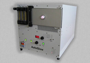
The AutoGlow 200 plasma/RIE system was used to perform this task with the following conditions:
- AutoGlow 200 in the RIE mode (with sample resting on the bottom power plate with the ground plate above).
- Pressure 550 mTorr
- 90% SF6
- 10% O2
- 100 watts
- 5 min
 for RIE Removal for Failure Analysis")
AutoGlow 200 chamber in RIE mode
Picture below: We ran a piece of a nitride on a broken silicon wafer to confirm the nitride etch. See attached picture showing yellowish looking nitride wafer piece (before), and after etch picture showing removal of the nitride (looks clear or white). Showed success with plasma Etching of silicon nitride (Si3N4) with RIE removal for failure analysis.
 for RIE Removal for Failure Analysis")
Test to confirm removal of nitride
 for RIE Removal for Failure Analysis")
EDS graph showing oxygen, aluminum and silicon. Note: no nitrogen peak
Graph above: After etching the samples, we had a local lab in Phoenix, AZ — Semtech Laboratories inspect the samples for nitrogen with EDS. https://semteclaboratories.com/about
Analysis confirms that the Si3N4 was removed.
Semtech reports: 250s count at about 2kcps. Could not find nitrogen, which shows removal of the Si3N4 (according to our Customer). Spectrum attached (see above). The first peak at about 0.5kev, is oxygen, second peak is aluminum, and the third peak is silicon. 250 seconds and 1000 counts per second.
The AutoGlow 200 is a very economical plasma/RIE system that can be used for removing nitride and oxide layers for FA and other applications.
We have a Customer in Europe, Texplained, that uses the AutoGlow 200 for removing films for Failure Analysis. Oliver Thomas, president of Texplained, recently presented at Hardwear.io USA 2025: Making IC Supply Chain Validation Easier For Open-Source Silicon Here is a video of the presentation by Oliver Thomas: https://www.youtube.com/watch?v=srbeubi005U
Here is a list of the equipment and process that Texplained uses for Failure Analysis (including the AutoGlow 200):
We are happy to share with you Le Lab, our webpage introducing our R&D-driven laboratory dedicated to extracting hidden information from integrated circuits (IC). On this webpage you will discover:
- Our process, step by step, explained from packaging and delayering to imaging and advanced extraction & active analysis.
- Our machines, as we benefit from advanced tools enabling precise access to IC layers, high-resolution imaging, and controlled interaction with semiconductor structures.
If you’re interested in understanding how we combine methodology, technology, and expertise to tackle complex hardware challenges, this page is worth exploring. https://texplained.com/lab/?utm_source=brevo&utm_campaign=Mars_copy&utm_medium=email
Should you want to contact Texplained, their web site is: https://texplained.com/
Click here for more information on the AutoGlow 200/300 used for FA: https://www.glowresearch.org/autoglow-plasma-system/
Click here for more information on FA plasma etching: https://www.glowresearch.org/plasma-applications/plasma-etching-passivation-nitride-and-oxide-failure-analysis/
AutoGlow 200/300 can process up to 8″ wafers