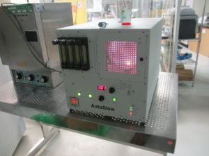
Plasma Etching Graphene with a Glow Research AutoGlow. A 5.97 um channel of Graphene was etched away in the trenches to create an insulated region of Sio2 around the channel and graphene pads.
Electrical Characterization of 2D Materials, Zainab Mahmood, Brandon Walter, Zhizhen. Ma, Dr. Y. lilach, Dr. V. Sorger, Dr. S. LeBlanc. See this paper here.
This paper comes from George Washington University: Department of Biomedical Engineering, Department of Electrical and Computer Engineering, Nanofabrication and Imaging Center, Department of Mechanical and Aerospace Engineering.
To see the poster click here.
Here are some notes from there good work:
The objective of this research was to electrically characterize graphene, a 2D material, by first fabricating graphene channels to eventually measure and calculate resistivity and electron mobility. Graphene’s unique electrical properties and its unusualy high electron mobility could lead to the development of flexible, high-speed electronics.
To measure the resistivity of graphene, a channel was created for current to flow directly between contacts at different channel lengths and widths. This channel was 5.97 um wide. The Glow Research AutoGlow was used for etching or removing the Graphene.

Quartz Chamber AutoGlow
